- 您现在的位置:买卖IC网 > Sheet目录3886 > PIC16C54C-04I/SO (Microchip Technology)IC MCU OTP 512X12 18SOIC
PIC18F2450/4450
DS39760A-page 172
Advance Information
2006 Microchip Technology Inc.
15.4.2
EUSART SYNCHRONOUS SLAVE
RECEPTION
The operation of the Synchronous Master and Slave
modes is identical, except in the case of Sleep or any
Idle mode and bit SREN, which is a “don’t care” in
Slave mode.
If receive is enabled by setting the CREN bit prior to
entering Sleep or any Idle mode, then a word may be
received while in this low-power mode. Once the word
is received, the RSR register will transfer the data to the
RCREG register. If the RCIE enable bit is set, the
interrupt generated will wake the chip from the low-
power mode. If the global interrupt is enabled, the
program will branch to the interrupt vector.
To set up a Synchronous Slave Reception:
1.
Enable the synchronous master serial port by
setting bits SYNC and SPEN and clearing bit
CSRC.
2.
If interrupts are desired, set enable bit RCIE.
3.
If 9-bit reception is desired, set bit RX9.
4.
To enable reception, set enable bit CREN.
5.
Flag bit RCIF will be set when reception is
complete. An interrupt will be generated if
enable bit RCIE was set.
6.
Read the RCSTA register to get the ninth bit (if
enabled) and determine if any error occurred
during reception.
7.
Read the 8-bit received data by reading the
RCREG register.
8.
If any error occurred, clear the error by clearing
bit CREN.
9.
If using interrupts, ensure that the GIE and PEIE
bits in the INTCON register (INTCON<7:6>) are
set.
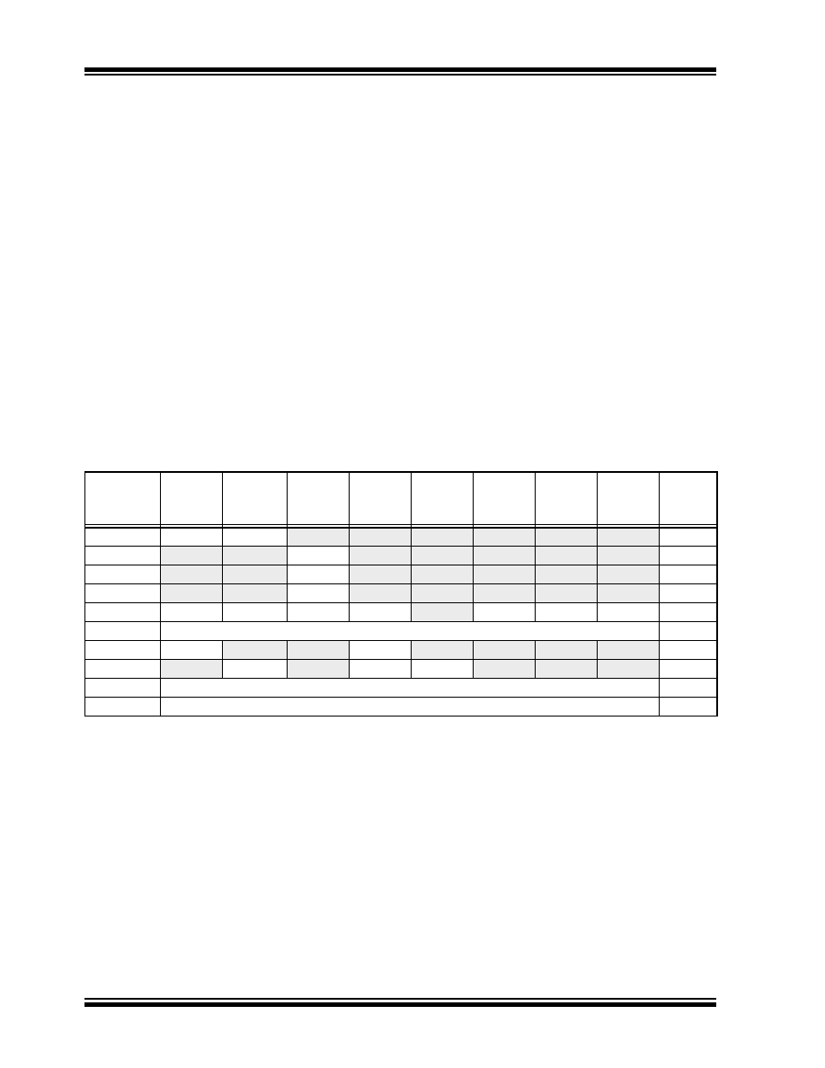
TABLE 15-10: REGISTERS ASSOCIATED WITH SYNCHRONOUS SLAVE RECEPTION
Name
Bit 7
Bit 6
Bit 5
Bit 4
Bit 3
Bit 2
Bit 1
Bit 0
Reset
Values
on page
INTCON
GIE/GIEH PEIE/GIEL
TMR0IE
INT0IE
RBIE
TMR0IF
INT0IF
RBIF
PIR1
—
ADIF
RCIF
TXIF
—
CCP1IF
TMR2IF
TMR1IF
PIE1
—
ADIE
RCIE
TXIE
—
CCP1IE
TMR2IE
TMR1IE
IPR1
—
ADIP
RCIP
TXIP
—
CCP1IP
TMR2IP
TMR1IP
RCSTA
SPEN
RX9
SREN
CREN
ADDEN
FERR
OERR
RX9D
RCREG
EUSART Receive Register
TXSTA
CSRC
TX9
TXEN
SYNC
SENDB
BRGH
TRMT
TX9D
BAUDCON
ABDOVF
RCIDL
—SCKP
BRG16
—
WUE
ABDEN
SPBRGH
EUSART Baud Rate Generator Register High Byte
SPBRG
EUSART Baud Rate Generator Register Low Byte
Legend: — = unimplemented, read as ‘0’. Shaded cells are not used for synchronous slave reception.
发布紧急采购,3分钟左右您将得到回复。
相关PDF资料
PIC16C54C-04/SO
IC MCU OTP 512X12 18SOIC
PIC16F722-I/ML
IC PIC MCU FLASH 2KX14 28-QFN
PIC16LCE623T-04I/SO
IC MCU CMOS.5K OTP W/EEPRM18SOIC
PIC16HV540-04I/SO
IC MCU OTP 512X12 18SOIC
PIC16LCE623T-04E/SS
IC MCU CMOS.5K OTP W/EEPRM20SSOP
PIC16LCE623T-04E/SO
IC MCU CMOS.5K OTP W/EEPRM18SOIC
5-520415-4
CONN TRIOMATE 4POS VERT TIN
6-176982-6
CONN TRIO-MATE 16POS .100 FFC
相关代理商/技术参数
PIC16C54C-04I/SO
制造商:Microchip Technology Inc 功能描述:8BIT CMOS MCU SMD 16C54 SOIC18
PIC16C54C-04I/SO
制造商:Microchip Technology Inc 功能描述:Microcontroller IC Number of I/Os:12
PIC16C54C-04I/SS
功能描述:8位微控制器 -MCU .75KB 25 RAM 12 I/O 4MHz IndTemp SSOP20 RoHS:否 制造商:Silicon Labs 核心:8051 处理器系列:C8051F39x 数据总线宽度:8 bit 最大时钟频率:50 MHz 程序存储器大小:16 KB 数据 RAM 大小:1 KB 片上 ADC:Yes 工作电源电压:1.8 V to 3.6 V 工作温度范围:- 40 C to + 105 C 封装 / 箱体:QFN-20 安装风格:SMD/SMT
PIC16C54C-20/P
功能描述:8位微控制器 -MCU .75KB 25 RAM 12 I/O 20MHz PDIP-18 RoHS:否 制造商:Silicon Labs 核心:8051 处理器系列:C8051F39x 数据总线宽度:8 bit 最大时钟频率:50 MHz 程序存储器大小:16 KB 数据 RAM 大小:1 KB 片上 ADC:Yes 工作电源电压:1.8 V to 3.6 V 工作温度范围:- 40 C to + 105 C 封装 / 箱体:QFN-20 安装风格:SMD/SMT
PIC16C54C-20/P
制造商:Microchip Technology Inc 功能描述:IC 8BIT CMOS MCU 16C54 DIP18
PIC16C54C-20/SO
功能描述:8位微控制器 -MCU .75KB 25 RAM 12 I/O 20MHz SOIC18 RoHS:否 制造商:Silicon Labs 核心:8051 处理器系列:C8051F39x 数据总线宽度:8 bit 最大时钟频率:50 MHz 程序存储器大小:16 KB 数据 RAM 大小:1 KB 片上 ADC:Yes 工作电源电压:1.8 V to 3.6 V 工作温度范围:- 40 C to + 105 C 封装 / 箱体:QFN-20 安装风格:SMD/SMT
PIC16C54C-20/SS
功能描述:8位微控制器 -MCU .75KB 25 RAM 12 I/O 20MHz SSOP20 RoHS:否 制造商:Silicon Labs 核心:8051 处理器系列:C8051F39x 数据总线宽度:8 bit 最大时钟频率:50 MHz 程序存储器大小:16 KB 数据 RAM 大小:1 KB 片上 ADC:Yes 工作电源电压:1.8 V to 3.6 V 工作温度范围:- 40 C to + 105 C 封装 / 箱体:QFN-20 安装风格:SMD/SMT
PIC16C54C-20E/P
功能描述:8位微控制器 -MCU .75KB 25 RAM 12 I/O 20MHz ExtTemp PDIP18 RoHS:否 制造商:Silicon Labs 核心:8051 处理器系列:C8051F39x 数据总线宽度:8 bit 最大时钟频率:50 MHz 程序存储器大小:16 KB 数据 RAM 大小:1 KB 片上 ADC:Yes 工作电源电压:1.8 V to 3.6 V 工作温度范围:- 40 C to + 105 C 封装 / 箱体:QFN-20 安装风格:SMD/SMT